|
BLILEY NV47M1008 Destructive Teardown Recently, I purchased
a Tindie OCXO 10 MHz board that was fully populated
and calibrated. My intention was to use it to supply not only the 10 MHz
square wave the board generated, but also to feed the square wave into a
buffer/filter circuit I designed, which outputs a 10 MHz sine wave. While
testing the circuit, I inadvertently touched the Tindie
board to part of a power supply generating 5V and 12V from 110 AC.
This catastrophically damaged the board. After interacting with
Chris from Analysir, which
developed the board, I determined that the damaged component on the board
was the OCXO module, which in my case was a BLILEY NV47M1008. I purchased a new Tindie
board and also bought off Ebay an additional
BLILEY module. This meant I had no use for
the damaged BLILEY module. Consequently, I decided to take it apart. I knew
from the outset that disassembling the module was going to be a
destructive teardown, since it encased its electronics in a sealed
metal case. So, I decided to document the teardown photographically and put
the pictures up on this web site in case others were curious what the
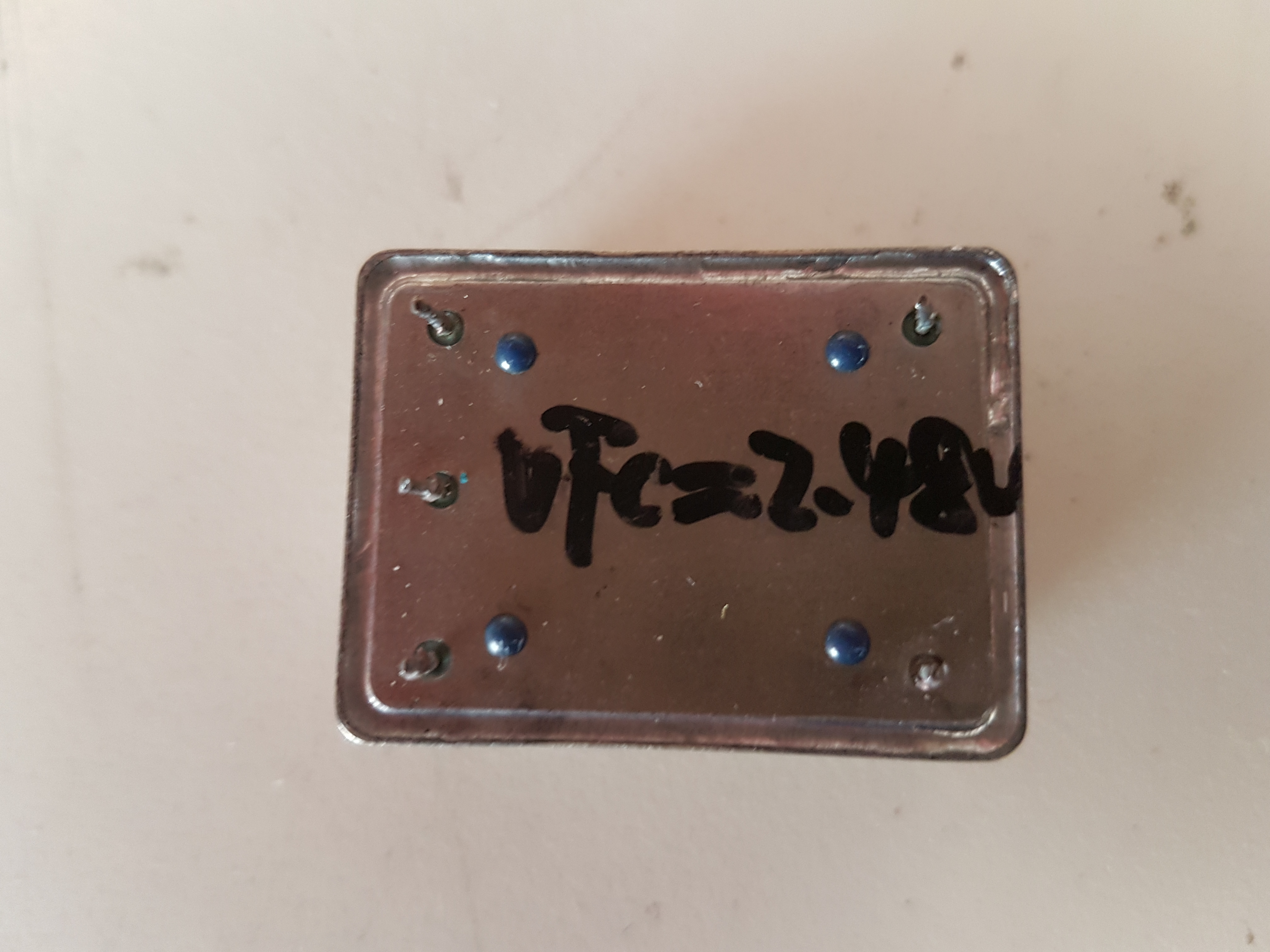
internals of such a module comprised. Figure 1 shows the bottom of the module with
5 pins (only 4 are functional): 2 serving to supply 5V and Ground; 1
returning the 10MHz square wave; and 1 accepting a reference voltage (Vref) that is used to fine tune the frequency of the
output - see NV47M1008 spec. (Note: the 4 blue dots on the
bottom are not pins. They are part of the bottom plate itself. The 5 pins
are on the left and right of the plate near the edge.)
Figure 1 - Bottom of BLILEY module. Figure 2 shows the
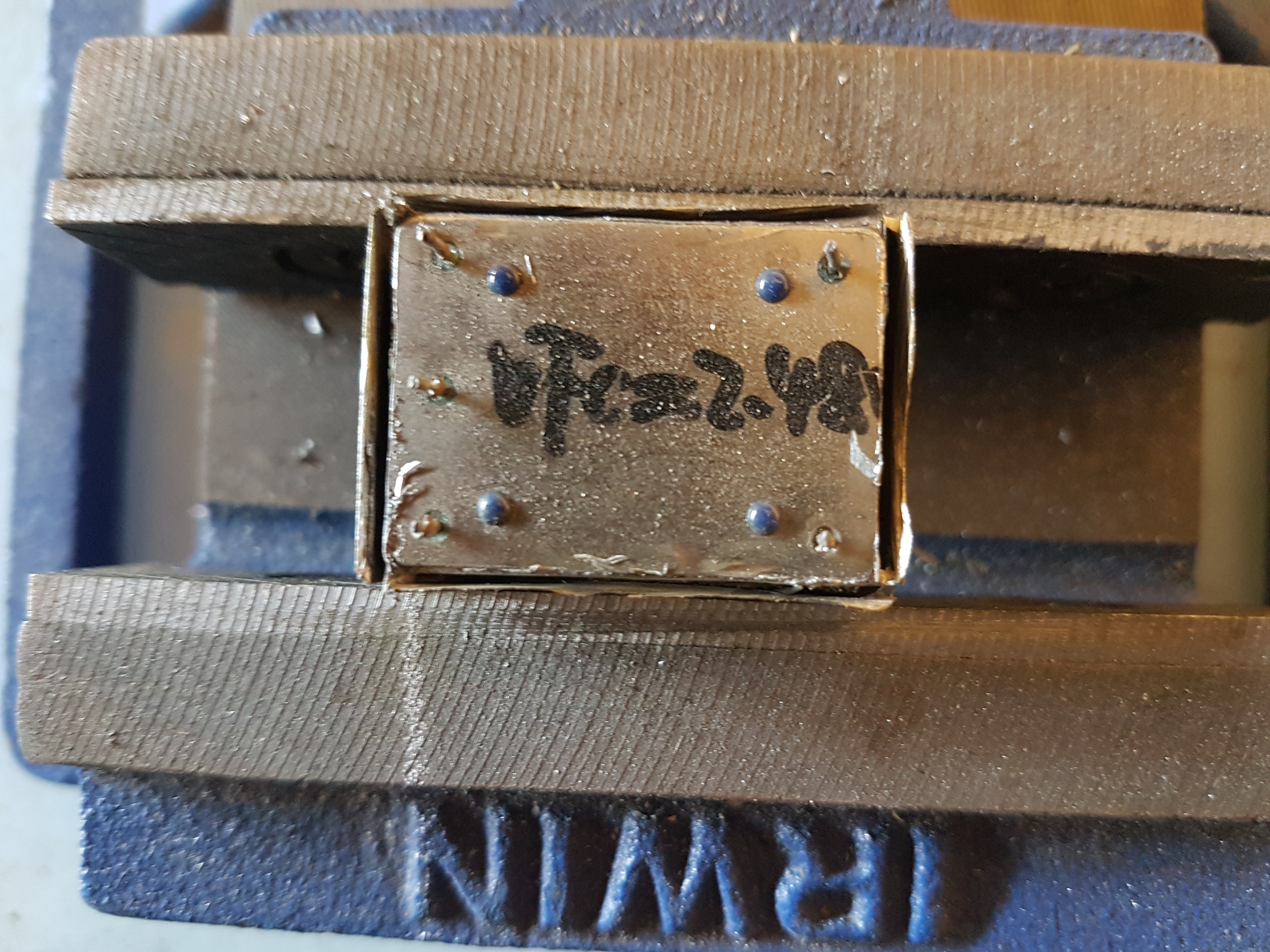
bottom of the module after I used a Drexel tool with a cutting disk to
remove the seal between the bottom plate and containing box. The seal was
not solder; rather it was a weld, which required significant pressure to
remove (I destroyed one cutting disk during the process).
Figure 2 - Weld
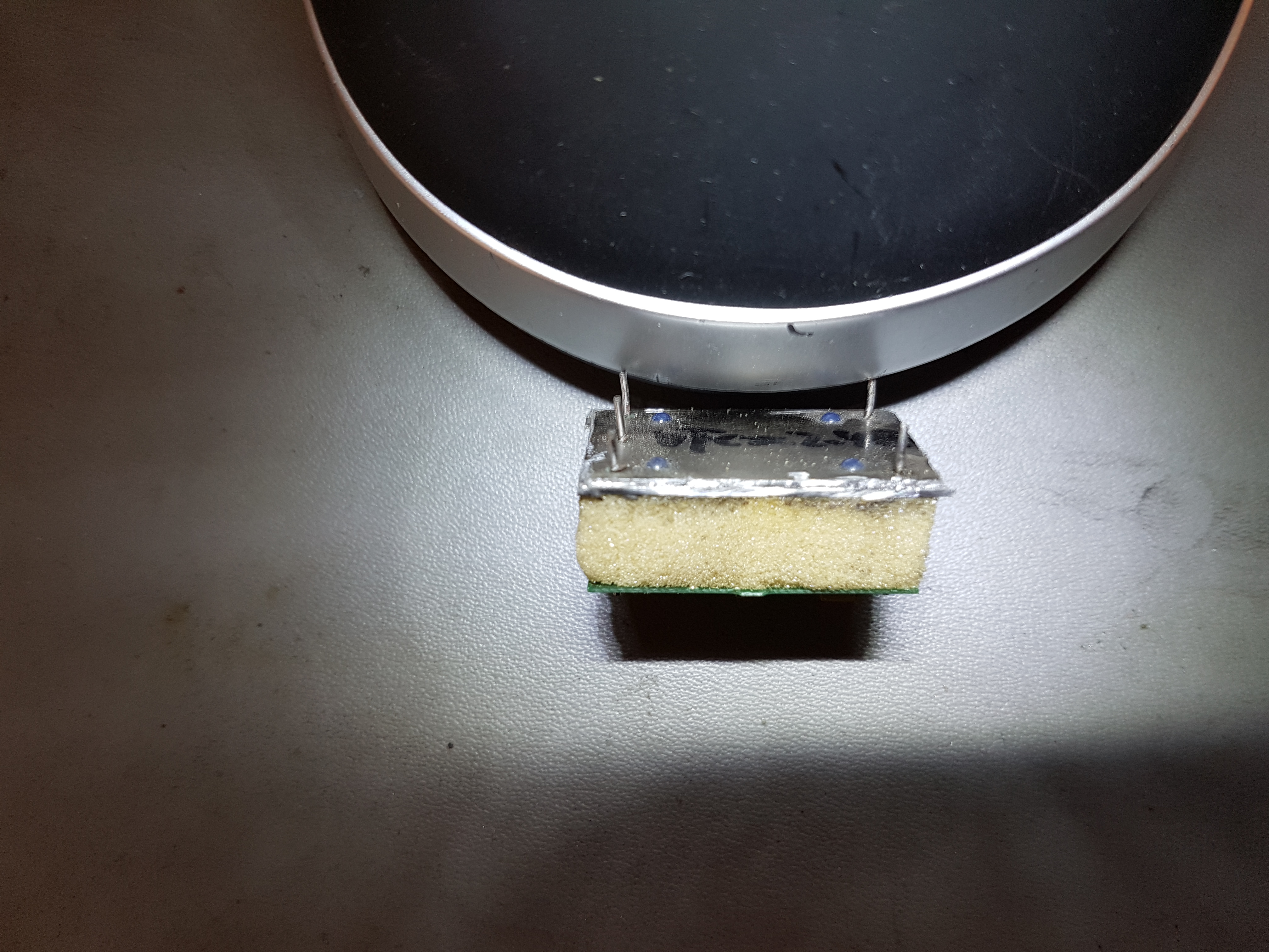
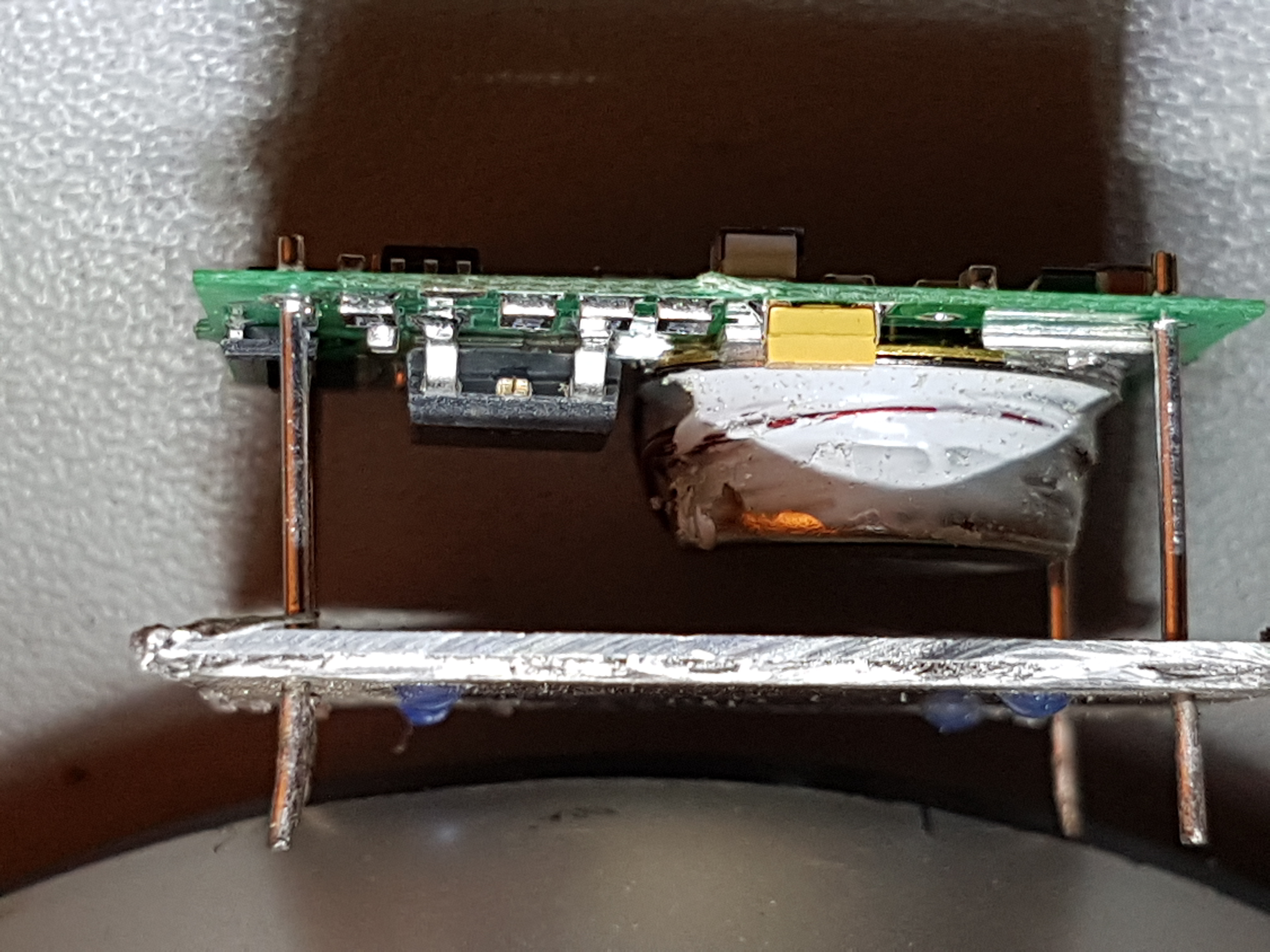
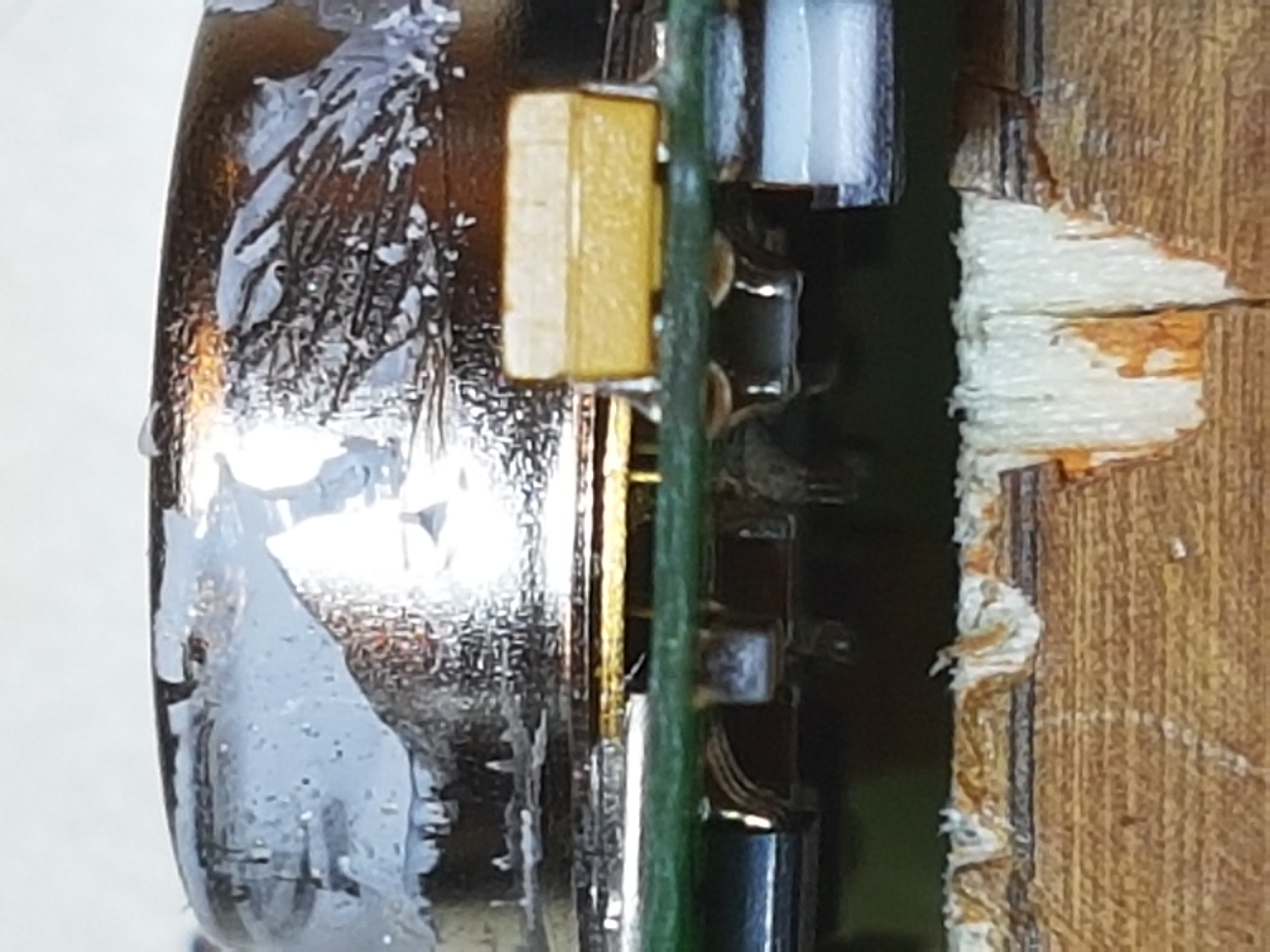
between bottom of module and metal can removed. Figure 3 shows the
board located on the other side of the module bottom plate. Note the
insulation in the cap that keeps the board from electrically contacting its
metal top. Also, just visible, is insulation between the board and the
bottom plate.
Figure 3 -
Electronics in module with insulation protecting it from the metal cap and
bottom plate Figure 4
shows more clearly the insulation between the PC board and the
bottom plate.
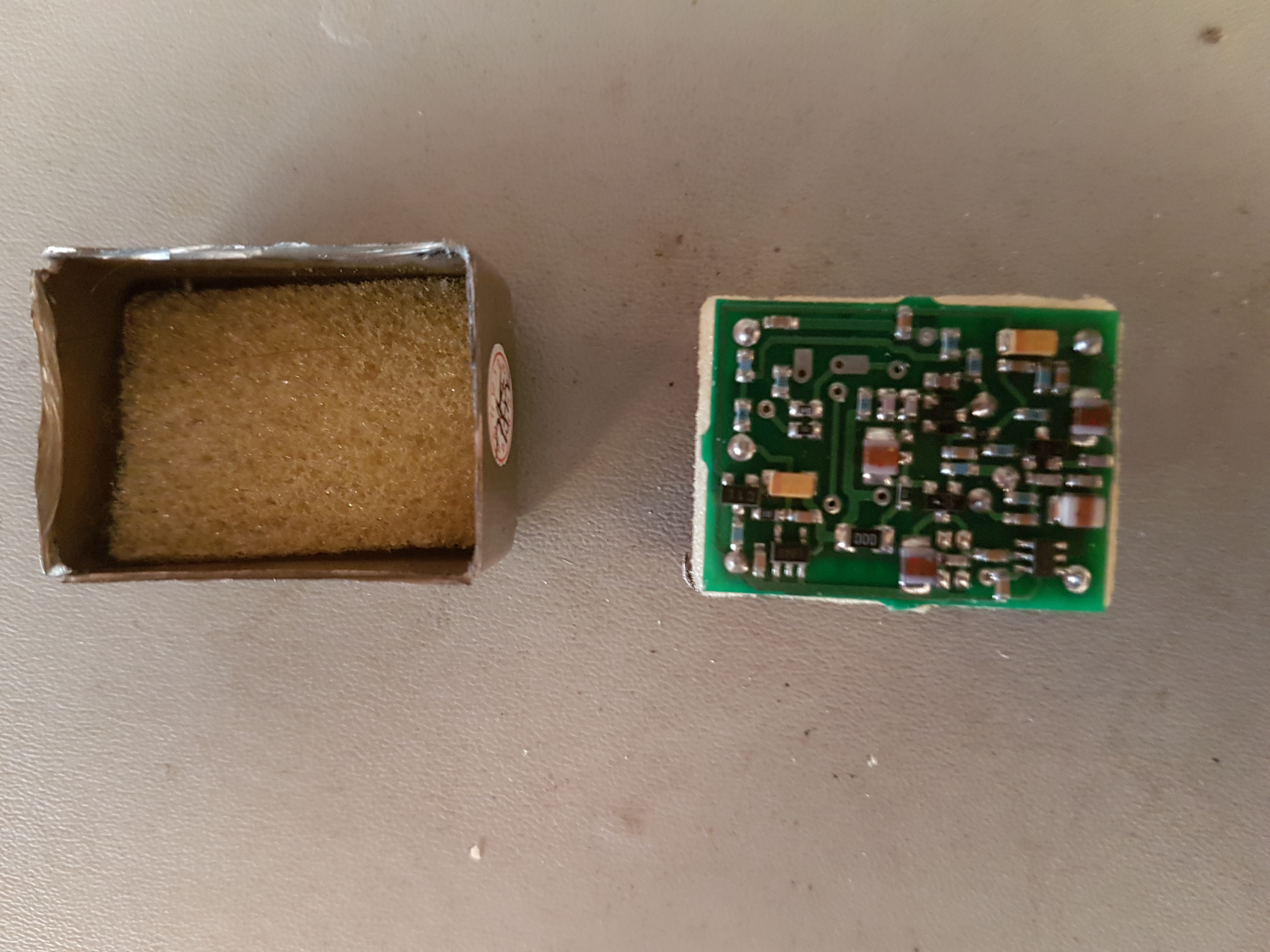
Figure 4 - Insulation
between bottom plate and PC board. Figure 5 shows the
same substructure with the insulation removed, revealing the components on
the PC board.
Figure 5 - Insulation
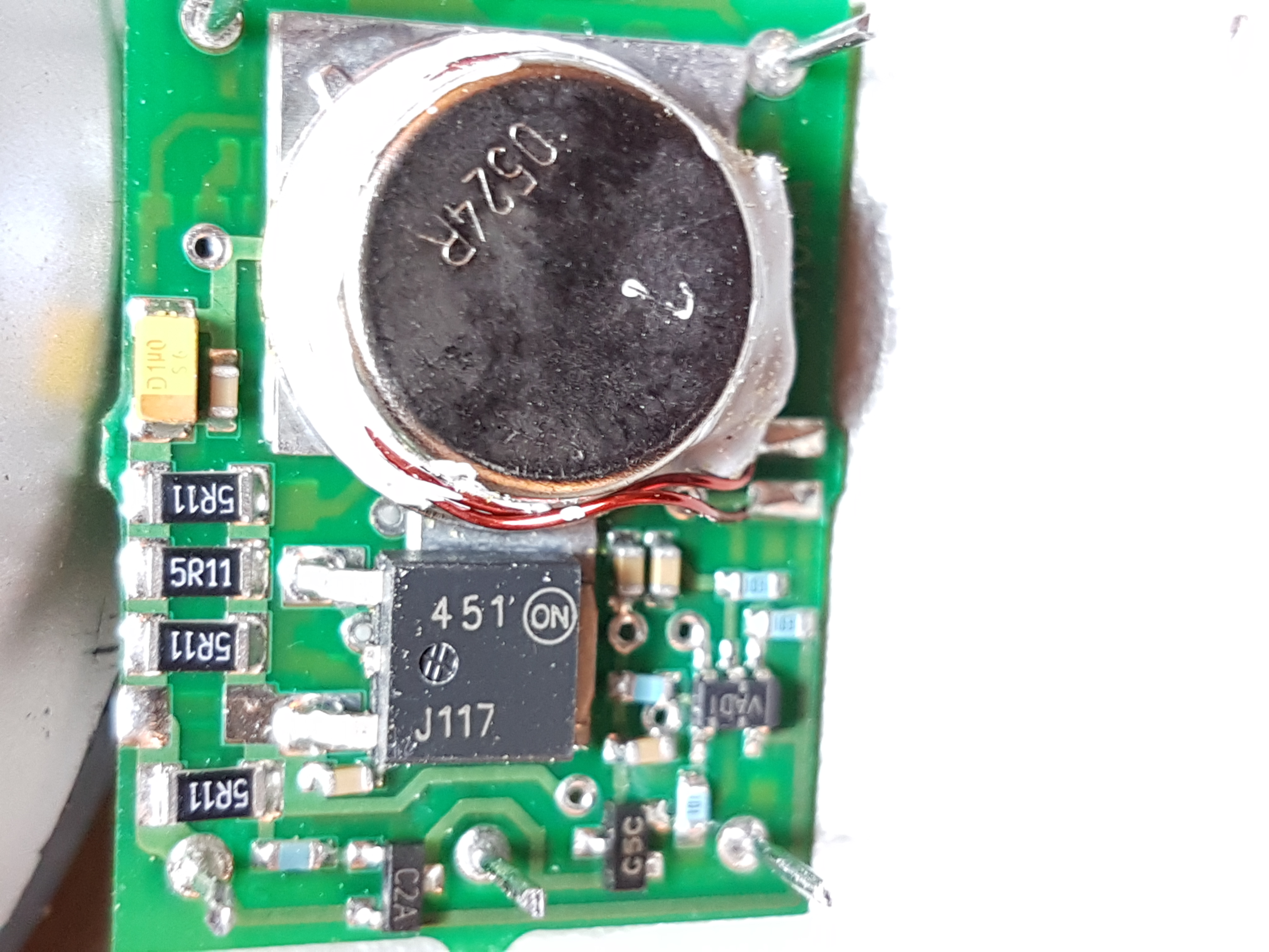
between PC board and bottom plate removed. Figure 6 shows the
top of the PC board. Note the oven can (the circular device labeled 052r4 on
top and with white sides comprising potting material). The chip next to it
labeled J117 might be a MJD117 (thanks to Damianos, who first
proposed this on the EEVBlog here), which is a darlington
pair. Chris noted that there is a lot of filtering on the board (see next
figure).
Figure 6 - Top of PC
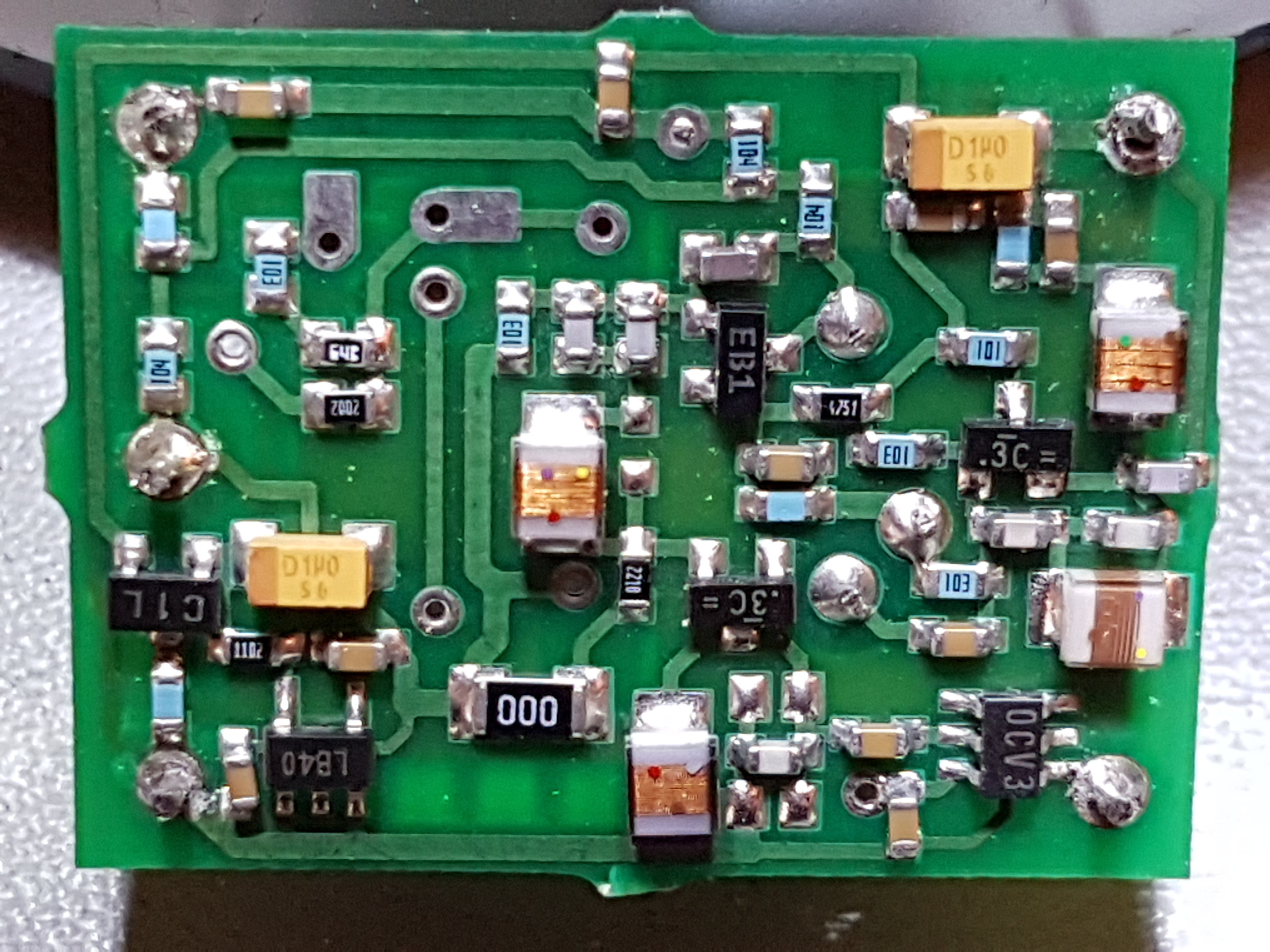
board Figure 7 shows the
bottom of the PC board. There is a 6-pin chip labeled OCV3 that may be a
Bliley proprietary part, since I could find no information about it on the
web. However, the name suggests something like "Oven Controlled Voltage
..." (Oven Controlled Voltage 3.3V - a voltage regulator?) There are
also chips labeled LB40 (5 pin) and C1L (3 pin), .3 C (3 pin) and EB1 (3
pin). The LB40 is a MIC5205-4.0 low noise low drop out voltage regulator
(noted by gamalot on the EEVBlog
forum here). The others are unknown.
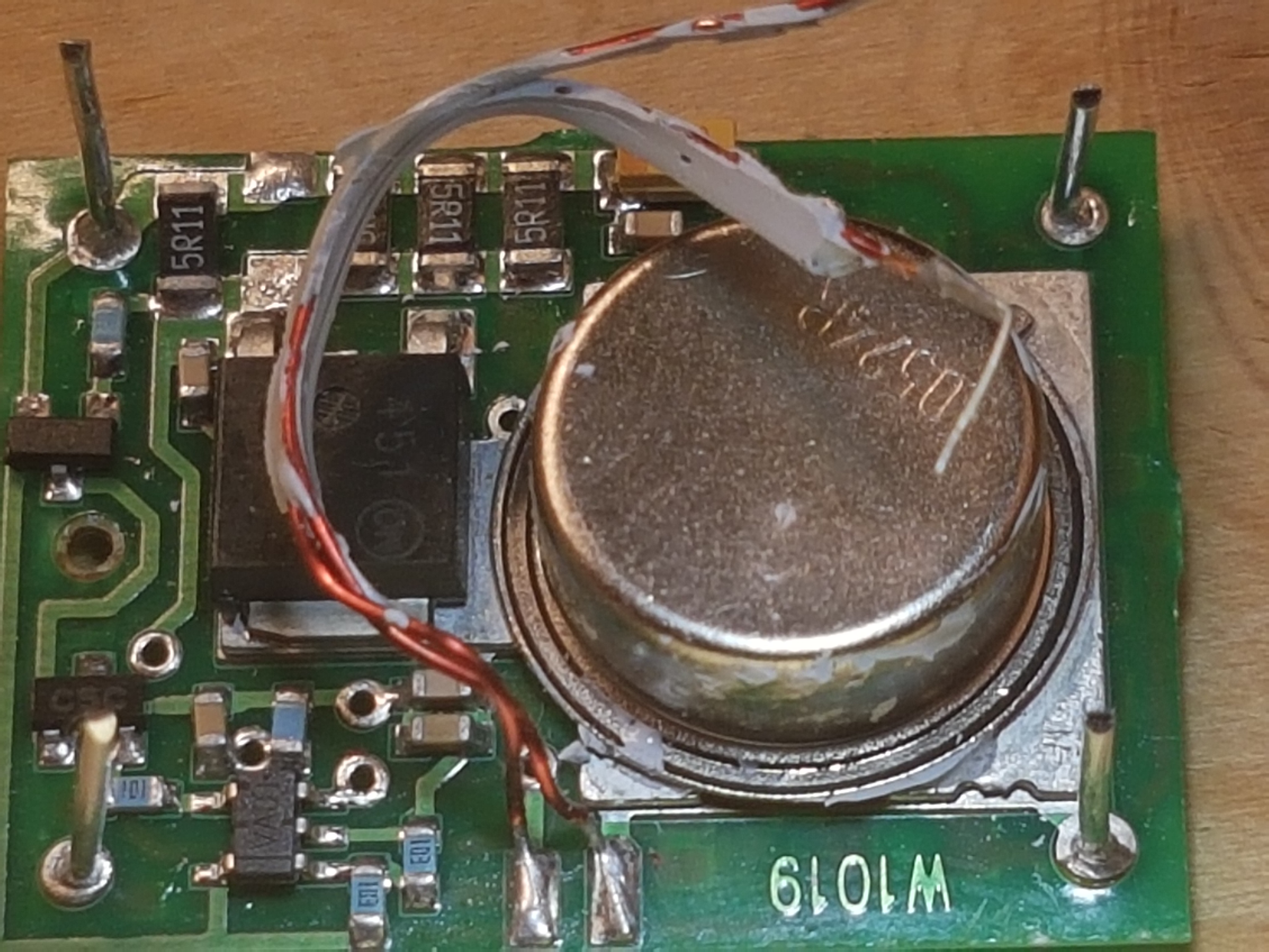
Figure 7 - Bottom of PC board. Figure 8 shows the
oven can with the white potting material removed. This material held the two
copper wires to the body of the can. The thin wires at the end probably
connected the copper wires to a thermistor, which was destroyed when I
removed the potting material.
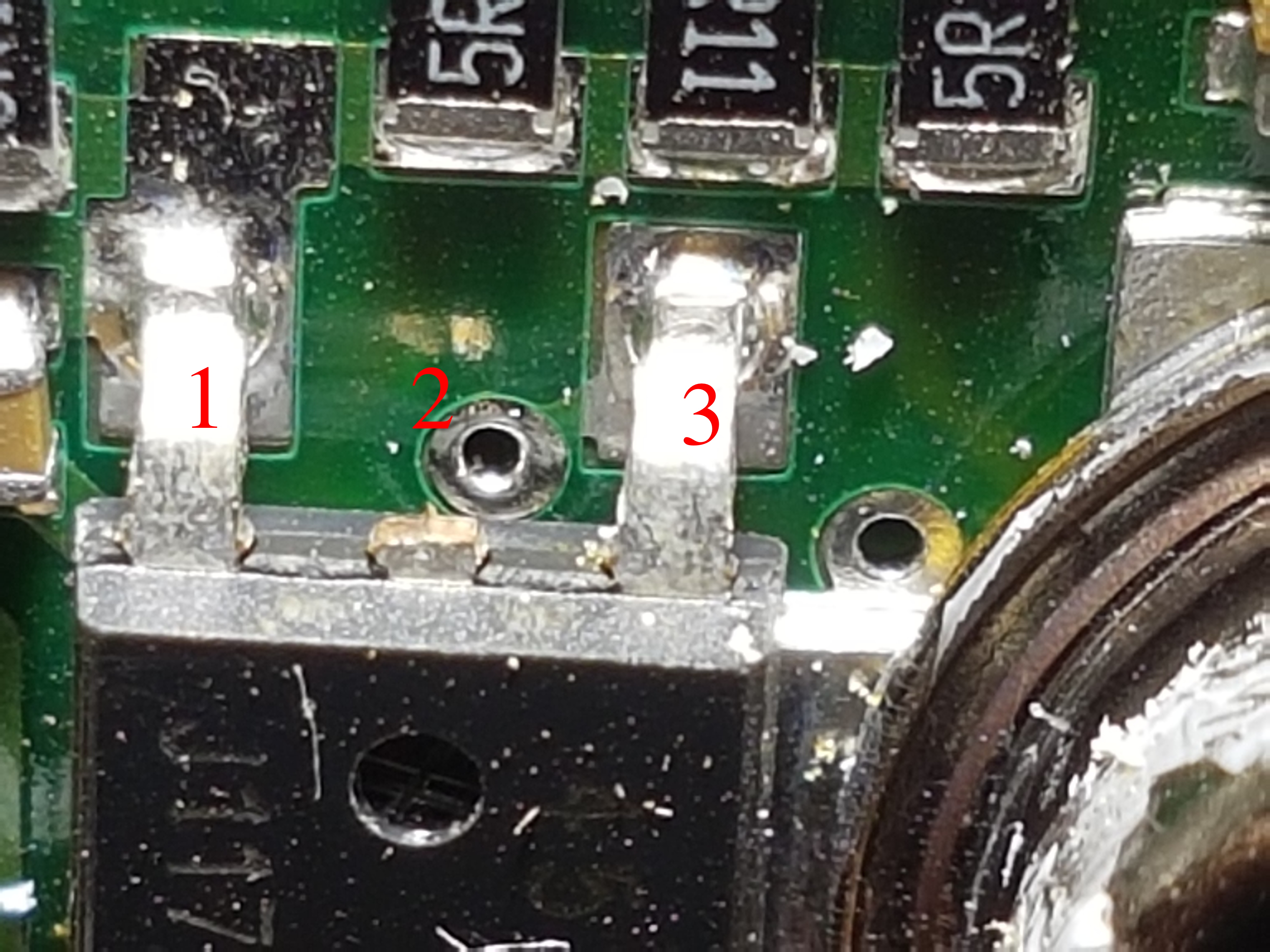
Figure 8 - Potting material removed from Oven Can Figure 9 shows the
area between the PC board and the can. Just barely visible between them
are pins that are soldered to pads on the bottom of the board.
Figure 9 - Area
between can and PC board. Is the device labeled
J117 a mosfet (2SJ117) or a PNP darlington pair (MJD117)? Figure 10 shows the device up
close. Notice the middle lead is either broken off or missing. The schematic of a MDJ117 in the DPAK case 369C
shows the middle pin missing, as in the picture. However, the code above the
MDJ117 designation (451) comprises 3 numbers (YWW), but according to the
spec, it should be 4 numbers (AYWW), where A signifies the assembly
location, Y the year and WW the work week. In addition, the middle lead
looks like it is sheared off, which would suggest it is not the DPAK case.
So, it is probably the DPAK-3 369D case with the middle lead sheared off.
Since the device is in circuit, measuring the voltages across the leads to
attempt to distinguish between a 2SJ117 or MJD117 is problematic. But, for
the record here are values (using a DMM in diode mode):
Figure 10 - J117 up
close. |